Nearly 20 years after building this project and documenting it here, I made a series of YouTube videos documenting the construction of it. You can find the YouTube playlist here.
After making a 6502-based single-board computer to make a cute little pattern of alternately on and off LEDs, you may be up for something a little more visually capable. To that end, this project straps an industry-standard graphical LCD to a 6502 system and allows you to display things on it. Although this project is still pretty simple and doesn't draw anything more than three bars on the display, the beauty of it is that you can draw anything you want, simply by re-programming the ROM chip. Just as with more complicated and modern computers, the hardware is just a framework, from which you can do just about anything imaginable through software.
Although much (most) of the wiring involved in this project duplicates what was already done in the first 6502 project, the text for those parts of the assembly will be repeated here; For the sake of completeness, this project does not assume that you have done and understood the first project, so you can take this project alone and begin with it if you so wish.
As you put this project together, you will need some way to hold the parts together and connect them, while keeping everything (including the wires) in place so they don't flop around. That's what the breadboard is for. Get the biggest breadboard you can find; Trust me, when you start building projects like this, you'll be glad for the extra space eventually. For this project, I recommend you put the CPU in the center, and the ROM and the VIA on either side of the CPU. This is because the ROM does not have any connections to the VIA, but the CPU has plenty of connections to both of them; This way, you will reduce how much you have to extend your wiring.
The industry-standard pin-numbering scheme for DIPs is to place pin 1 in the upper-left corner, and begin moving down, until you reach the half-way pin in the lower-left corner. From there, move to the right side and move back up, ending up with the highest-numbered pin in the upper-right corner. For example, on a 40-pin chip, pin 1 is in the upper-left corner, pin 20 is in the lower-left corner, pin 21 is in the lower-right corner, and pin 40 is in the upper-right corner. Note that this requires knowing which side is "up" on the chip; Most chips are manufactured with a small orienting notch carved into one side. This notch is meant to be at the top in all pin diagrams.
Let's start with the centerpiece of the computer, the CPU. As has been mentioned, for this project we're using the classic 6502 CPU. In terms of non-Intel CPU platforms, this CPU probably stands next to the Motorola 6800-series as the most-used for microcomputer platforms. The pinout for this CPU is as follows:
1: Vss (Ground)
2: RDY
3: CLK1 (Out)
4: /IRQ
5: NC (Not Connected)
6: /NMI
7: SYNC
8: Vcc (+5V)
9: A0
10: A1
11: A2
12: A3
13: A4
14: A5
15: A6
16: A7
17: A8
18: A9
19: A10
20: A11
21: Vss (Ground)
22: A12
23: A13
24: A14
25: A15
26: D7
27: D6
28: D5
29: D4
30: D3
31: D2
32: D1
33: D0
34: R/W
35: NC (Not Connected)
36: NC (Not Connected)
37: CLK0 (In)
38: SO
39: CLK2 (Out)
40: /RES
The 6502 has, weirdly enough, three power pins; One positive voltage-in and two ground pins. Connect all three (1 and 21 to ground, and 8 to +5 V DC) to give your CPU power.
Make sure that RDY (Ready, which is pin 2) is tied high, or else you might have problems with the CPU halting later. Also tie /IRQ and /NMI high through 3K-ohm resistors. (The official documentation for the 6502 specifies 3K pull-up resistors for these pins.) There is some controversy attached to pin 38, the SO (Set Overflow) pin; It simply sets the overflow register inside the CPU. It doesn't seem to make much difference regarding operation of the CPU, and I used to recommend leaving it unconnected. This is what I did when I made my projects, and they worked fine, but in digital design, it's never a good idea to leave a digital input unconnected, because then the pin will float and could cause unpredictable behavior inside the chip. The SO pin is active-low, so go ahead and connect pin 38 to the high side of the power supply so it stays inactive. (Thanks to Roy J. Tellason for pointing out to me the folly of leaving a digital input unconnected.)
The clock pins of the 6502 are interesting beasts. However, the only one that you really need to concern yourself with right now is pin 37, which is the only clock input on the 6502. Every CPU chip has a clock pin, and this pin is simply a trigger for the CPU: Every time the clock input pulses, the CPU performs a cycle (which basically means it runs an instruction). That's right, the speed of the CPU is externally-controlled. You can run the CPU as fast or as slow as you want to, simply by changing how fast the CLK pin pulses up and down, although if you make it too high, the CPU will stop being able to keep up and may overheat from trying too hard. This is why every CPU in the world has a hertz rating, which is how fast it can handle clock pulses before it stops working reliably. You can go under this speed by simply lowering your clock pulse, but you can't go much over it without risking damage to the CPU.
The clock input can be a little difficult to generate if you're not familiar with analog electronics. Because the timing of it is so precise, you cannot simply manually cycle the clock by flipping it from low to high with a switch. Doing this will make a split-second instability during each transition, because whenever you press or release a hand-operated switch, the circuit state does not go instantly from low to high, or high to low; Rather, it fluctuates between them for just a fraction of a second. Although it doesn't seem like a long time to you, the clock input of a CPU is so sensitive that trying to pulse it by hand will make the CPU crash instantly. (This behaviour of switches is called "switch bounce", and is an inescapable fact of life when working with switches in electronics.)
So what must you do with this clock input? You need to supply it with a good clean square wave, which is an electric signal which rises and falls instantly (or pretty close to instantly). This creates a waveform which looks like a series of three-sided squares or rectangles, hence its name:
�������Ŀ �������Ŀ �������Ŀ
� � � � � �
� � � � � �
� � � � � �
� � � � � �
� � � � � �
������� �������� �������� ��������
The creation of square-wave clock signals is a whole world of a topic unto itself. As such, it is out of the scope of this file; For now, a very quick cook-book recipe for making a square wave suitable for use with a CPU like the 6502 is as follows:
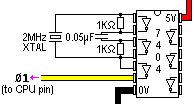
Take a 7404 chip, which is a typical TTL logic inverter. (You shold be able to use most variants, including 74F04, 74LS04, etc.) Power it up by connecting its pin 14 to +5 volts and pin 7 to ground. Connect pin 1 to pin 2 through a 1,000-ohm resistor. Also connect pin 1 to pin 4 through a 2 MHz two-pin crystal. Connect pin 2 to pin 3 through a 0.05 microfarad capacitor. Connect pin 3 to pin 4 through another 1,000-ohm resistor. Finally, connect pin 4 directly to pin 5. Pin 6 is now your clock output, and you can connect it directly to pin 37 on the 6502 CPU.
You may need to play around with this clock circuit a bit; However, it is the one specified by Harry The Bastard, who used to have a good website about the 6502 with this picture of the circuit I just described. His site was formerly at www.harry-the-b.demon.co.uk, then he got it moved to a dedicated domain name at www.harrythebastard.org. Unfortunately, harrythebastard.org seems to have been neglected, and the domain got snatched up by a company calling itself Ultimate Search, which seems to have nothing better to do than steal abandoned domain names to spread the virus of their ugly web directory. (Same problem that famously happened to Underdogs a while back.) You may wish to see if you have good results with a 1 MHz crystal, a different-rated capacitor, etc. However, this setup worked fine for me.
And now we come to the RESET pin. Like any CPU, the 6502 must be reset when it is first powered on. This is because as the power is first coming on, it goes through a transition state where the power is not quite fully on yet. This kind of marginal voltage confuses digital electronics, and so all CPUs must be immediately reset after they're turned on to clear them out and re-start them with the now-fully-established power. Desktop computers have built-in circuits which automatically reset the CPU when the power comes on, but for this project, we can stand to keep things simple by manually resetting the CPU with a button. Some would argue that resetting the CPU with a button creates the same variation problems that crop up when you try to clock-pulse the CPU with a button; However, this worked for me. Resetting the CPU with a button seems to work well enough. For this, I recommend one of those tiny push-button switches, the kind which are meant to be mounted on a printed circuit board. You can get them to fit on a breadboard too; They take up very little space and they work quite well. Use a momentary, normally-open push-button switch. (The "momentary" part means that it only takes effect when you push it, as opposed to a toggle switch, which flips back and forth each time you push it. The "normally-open" part means that it is not connected when it's not pushed.)
Begin by connecting the button to the 6502's RESET pin, and connecting the other side of the button to ground. This way, when you push the button, the RESET pin will go to ground, and since it is active-low, pushing the button will reset the CPU. But this leaves us with another interesting electronic problem: When we let go of the button, the RESET pin needs to go high. How can we make it do this? We could certainly just connect it directly to the high end of the power supply, but then when we pushed the button... Well, you can hopefully guess what would happen. We'd be connecting the two sides of the power supply directly together, which would result in a short-circuit. To deal with this problem, we'll use what is technically called a "pull-up resistor", a resistor used to keep something high when it will sometimes be connected directly to ground. Run a 3,000-ohm resistor from the 6502's RESET pin to the positive end of the power supply. Now, normally the resistor will keep the pin high, so the CPU does not reset. But when we push the button, the button provides a direct path to ground, and that direct path is stronger than the path to the high voltage (because there's a 3K-ohm resistor in the way), so we can reset the CPU without fear of it getting confused or short-circuiting.
That pretty much leaves us with the A and D pins of the CPU, which constitute the address bus and the data bus, respectively. The R/W and CLK2 pins also remain; We'll get to all of these in the appropriate sections of the parts decribing the other chips in this project.
As an afterthought, you may want to take a moment to add a capacitor to your CPU. This should simply be a capacitor connected directly between the positive and negative sides of the power supply, connected as close to the CPU as possible; This adds some stability to digital ICs, and generally you should have one on any CPU you use. (This is called a "decoupling capacitor".) The capacitor should be fast (i.e. have a low farad rating, somewhere from 0.1 to 4.7 microfarads), and it should prefereably be ceramic, although I used a mylar one.
For that added touch to your computer, you can add a reset IC, which is an ultra-simple IC which resets your CPU for you automatically. Essentially, a reset IC is a chip with three pins, two of which are simply connected to the power supply, and the third of which is a reset output. If for any reason the power wavers or is otherwise not appropriate for powering digital electronics (such as when the power supply is first powering up when you turn it on), the reset IC sends a reset signal out; When the power stabilizes, it releases the reset signal. It really is that simple. These reset ICs are very cheap and they eliminate the one step that you need to do to get your computer working (besides plugging it in). If you don't use such a device then you just need to reset the system manually with a switch every time you turn it on. I must admit that I thought this would be a problem with the 6502, because the reset button suffers from the same problems of switch bounce as a manual clock button would, and much has been said about "dirty" reset signals and how they tend to prevent CPUs from working properly. This was not such a problem with the Z80 projects, because they were clocked so low that the button's input rose and fell before a single clock cycle completed, but the 6502 must be clocked much faster, which could create a problem. In my experiment, however, I found the 6502 worked just fine with a manual push-button reset. If you're really concerned about reliability, a reset IC is not an expensive addition to your system.
You are now finished wiring your 6502 CPU chip.
(For my earlier quick-start guide to the 6502, click here.)
For this project, we're using a 2865 EEPROM chip, which is an 8-bit, 8-kilobyte, 28-pin ROM chip that can be easily programmed and re-programmed without special chip-erasing-and-burning hardware. It's also fairly inexpensive (mine was $5), making it a good choice for a small hobby project. The pinout for the 2865 is as follows:
1: READY/BUSY
2: A12
3: A7
4: A8
5: A5
6: A4
7: A3
8: A2
9: A1
10: A0
11: D1
12: D2
13: D3
14: Vss (Ground)
15: D4
16: D5
17: D6
18: D7
19: D8
20: /CE (Chip Enable)
21: A10
22: /OE (Output Enable)
23: A11
24: A9
25: A6
26: N.C. (Not Connected)
27: /WE (Write Enable)
28: Vcc (+5 Volts)
The very first thing you need to do with the ROM chip, before you can actually incorporate it into your circuit, is program it. For this project, we'll use a somewhat longer program than the first project used, so relax and take your time if you're programming the EEPROM by hand. Program your 2865 with the following byte values:
0000000000000: 10101001 (A9) ;LDA #$FF
0000000000001: 11111111 (FF)
0000000000010: 10001101 (8D) ;STA $8002
0000000000011: 00000010 (02)
0000000000100: 10000000 (80)
0000000000101: 10001101 (8D) ;STA $8003
0000000000110: 00000011 (03)
0000000000111: 10000000 (80)
0000000001000: 10101001 (A9) ;LDA #$06
0000000001001: 00000110 (06)
0000000001010: 10001101 (8D) ;STA $8000
0000000001011: 00000000 (00)
0000000001100: 10000000 (80)
0000000001101: 10101001 (A9) ;LDA #$3F
0000000001110: 00111111 (3F)
0000000001111: 10001101 (8D) ;STA $8001
0000000010000: 00000001 (01)
0000000010001: 10000000 (80)
0000000010010: 10101001 (A9) ;LDA #$07
0000000010011: 00000111 (07)
0000000010100: 10001101 (8D) ;STA $8000
0000000010101: 00000000 (00)
0000000010110: 10000000 (80)
0000000010111: 10101001 (A9) ;LDA #$06
0000000011000: 00000110 (06)
0000000011001: 10001101 (8D) ;STA $8000
0000000011010: 00000000 (00)
0000000011011: 10000000 (80)
0000000011100: 10101001 (A9) ;LDA #$0E
0000000011101: 00001110 (0E)
0000000011110: 10001101 (8D) ;STA $8000
0000000011111: 00000000 (00)
0000000100000: 10000000 (80)
0000000100001: 10101001 (A9) ;LDA #$B7
0000000100010: 10110111 (B7)
0000000100011: 10001101 (8D) ;STA $8001
0000000100100: 00000001 (01)
0000000100101: 10000000 (80)
0000000100110: 10101001 (A9) ;LDA #$0F
0000000100111: 00001111 (0F)
0000000101000: 10001101 (8D) ;STA $8000
0000000101001: 00000000 (00)
0000000101010: 10000000 (80)
0000000101011: 10101001 (A9) ;LDA #$0E
0000000101100: 00001110 (0E)
0000000101101: 10001101 (8D) ;STA $8000
0000000101110: 00000000 (00)
0000000101111: 10000000 (80)
0000000110000: 01001100 (4C) ;JMP $E026
0000000110001: 00100110 (26)
0000000110010: 11100000 (E0)
(The first number is the byte address on the chip, the second number is the actual data value that should be in that memory cell. The third number, in parentheses, is the hexadecimal value of the data byte, and the text after some of those bytes is just the assembly-language instructions, placed there for easy reference.) Remember that in this kind of binary work, bit numbers are read from right to left, so in the first byte (which is 10101001), pin D3 on the ROM chip should be 0, NOT 1, which is how it would be if the pins were numbered from left to right.) It is beyond the scope of this file to detail how to program an EEPROM chip; If you have one and don't know how, read my separate electronics writeup, How to program an EEPROM.
Below, the code is reproduced in 6502 assembly language. Here you can see exactly what the code is doing.
;Make all VIA's pins be outputs
LDA #$FF ;10101001 11111111 or A9 FF
STA $8002 ;10001101 00000010 10000000 or 8D 02 80
STA $8003 ;10001101 00000011 10000000 or 8D 03 80
;Put D/I low for instruction
LDA #$06 ;10101001 00000110 or A9 06
STA $8000 ;10001101 00000000 10000000 or 8D 00 80
;Put 3Fh into the accumulator, which is the "turn LCD on" command
LDA #$3F ;10101001 00111111 or A9 3F
;Put the accumulator on port 1, which is ORA
STA $8001 ;10001101 00000001 10000000 or 8D 01 80
;Toggle the LCD's Enable pin to make the command take effect
LDA #$07 ;10101001 00000111 or A9 07
STA $8000 ;10001101 00000000 10000000 or 8D 00 80
LDA #$06 ;10101001 00000110 or A9 06
STA $8000 ;10001101 00000000 10000000 or 8D 00 80
;LCD should now be on
;Put D/I high for data
LDA #$0E ;10101001 00001110 or A9 0E
STA $8000 ;10001101 00000000 10000000 or 8D 00 80
;D/I is now high
;Store 10110111 (B7h) (pixel pattern) in the accumulator
LDA #$B7 ;10101001 10110111 or A9 B7
;...And put it in ORA
STA $8001 ;10001101 00000001 10000000 or 8D 01 80
;Toggle LCD's Enable
LDA #$0F ;10101001 00001111 or A9 0F
STA $8000 ;10001101 00000000 10000000 or 8D 00 80
LDA #$0E ;10101001 00001110 or A9 0E
STA $8000 ;10001101 00000000 10000000 or 8D 00 80
;Keep toggling Enable infinitely
JMP $E026 ;01001100 00100110 11100000 or 4C 26 E0
There are two more bytes on the ROM that need to be coded for this project to work properly. They are located at addresses 1111111111100 (1FFCh) and 1111111111101 (1FFDh). Set address 1FFCh to 00h, and set address 1FFDh to E0h (which is 11100000 in binary).
After the chip is programmed, you can drop it onto your circuit board. Begin by powering it up (connecting it appropriately to your power supply via pins 28 and 14). Keep pin 27 (Write Enable) high, since that pin is only used to write to the ROM, and you do not want to overwrite this program that you worked so hard to get into it in the first place.
Connect the ROM's data bus to the CPU's data bus. This is basically a matter of simple name-matching with wires, EXCEPT for one small anomaly: The ROM's data bus pins are numbered beginning with 1, while the 6502 CPU's data bus is numbered beginning with 0, resulting in an off-by-one difference for each pin mating. Below is a table indicating where each pin on the CPU should meet each pin on the ROM (the CPU's pin is on the left, the ROM's pin is on the right):
D0 --- D1
D1 --- D2
D2 --- D3
D3 --- D4
D4 --- D5
D5 --- D6
D6 --- D7
D7 --- D8
Connect the ROM's address bus pins to the CPU in exactly the same way. However, because the ROM we're using only has 13 address bus pins and the CPU has 16, you can just leave the top three address bus pins of the CPU unconnected to the ROM. (Inexplicably, while the 2865 numbers its D pins beginning with 1, the A pins begin with 0 just as they do on the 6502, so you can match the names directly.)
Now all that's left on the 2865 is the CE (Chip Enable) pin and the OE (Output Enable) pin, which, when both activated, will make the ROM spit out whatever is in the selected memory address. These pins will be covered below, in the section on the 74LS138 3-to-8 decoder.
You are now finished wiring your 2865 ROM chip.
If you really want to cut down on the number of obscure parts you're using for this project, you can certainly omit the I/O chip and create your own I/O circuitry. All it really is is a buffer of the data bus, so you can set up some kind of glue logic that latches the data bus and maintains it on some other wires, but the I/O chip we're using is a fairly simple beast, and it will make things a lot easier on you later when you want multiple peripherals. Trust me, it's worth getting an I/O chip and learning to use it, it will make your life easier.
I'm a fan of the 6522 VIA (Versatile Interface Adapter) chip. It's simply and logically designed, yet quite powerful. It's fairly readily available and very cheap. And it was designed to work with the 6502 anyway, so it's a match made in heaven. (Or at least in the factory.)
The 6522's pinout is as follows:
1: Vss (Ground)
2: PA0
3: PA1
4: PA2
5: PA3
6: PA4
7: PA5
8: PA6
9: PA7
10: PB0
11: PB1
12: PB2
13: PB3
14: PB4
15: PB5
16: PB6
17: PB7
18: CB1 (Control for Port B)
19: CB2 (Control for Port B)
20: Vcc (+5V)
21: IRQ (Active-low; Output to the CPU, not an input to the VIA)
22: R/W (High = read, low = write)
23: CS2 (Chip Select 1; Active-low)
24: CS1 (Chip Select 2; Active-high)
25: CLK2 (Enable)
26: D7
27: D6
28: D5
29: D4
30: D3
31: D2
32: D1
33: D0
34: RES (Reset; active-low)
35: RS3 (Register Select 3)
36: RS2 (Register Select 2)
37: RS1 (Register Select 1)
38: RS0 (Register Select 0)
39: CA2 (Control for Port A)
40: CA1 (Control for Port A)
Ignore the CA and CB pins for this project; We won't be using them at all.
Begin by powering up the VIA by connecting pins 20 and 1 to your power supply as appropriate.
The RS pins on the VIA are normally connected to a CPU's address bus, and that's exactly what we're going to do here. Connect RS0 on the VIA to A0 on the 6502, RS1 on the VIA to A1 on the 6502, RS2 on the VIA to A2 on the 6502, and RS3 on the VIA to A3 on the 6502. Similarly, connect all the D pins to each other; This is just a matter of pin-name-matching, once again.
For the 6522 to work, both CS (Chip Select) pins must be active. The trick here is that CS1 is active-high and CS2 is active-low; So tie CS1 to the high side of your power supply, and we'll worry about CS2 when we get to the 74LS138 chip. Also tie R/W directly to the R/W pin on the CPU. Similarly, the CLK2 pin can be connected directly to the 6502's CLK2 output; See how easy things are when chips are made for each other?
Almost done! The 6522 has a reset pin, just like the CPU. Add a reset button to it, just like the CPU; Connect the pin to ground through the button, and add a 3,000-ohm pull-up resistor so the pin normally stays high.
Now all that's left is those PA and PB pins. Those pins are the actual I/O buses, the two I/O buses that are built into the 6522. For this project, we'll be using most of the pins to connect to the LCD. We'll cover them in more detail on the section for the LCD below.
You are now finished wiring your 6522 I/O chip.
(For my earlier introduction to the 6522, click here.)
For the ultra-simple Z80 projects which had no RAM (only ROM), it was not necessary to use a memory selection chip. In a "real" computer, however, it is necessary to have a mechanism to divide the RAM from the ROM. Although this computer does not have any RAM either, it suffers from an irritating aspect of the 6502: The 6502 requires "memory-mapped I/O", which means that it must have the I/O addresses actually mapped into the system memory space, which creates a "hole" in your memory which cannot be used for data storage because it's being used by your peripheral controllers(s). Since the 6502 treats your I/O chip as just another memory chip, we end up with two memory-mapped chips on this computer, and thus we need a way for the CPU to choose which is which.
That's where the memory decoder chip comes in. It is a rather simple, but useful device which has a number of inputs which are connected to the top of the CPU's address bus, and a number of outputs, one of which turns on depending on the state of the inputs. The number of outputs on such a chip is 2 to the power of X, where X is how many inputs there are. We're using a 74LS138 chip, which is a 3-to-8 decoder, meaning it has 3 inputs and 8 outputs. The pinout for the 74LS138 is as follows:
1: A0
2: A1
3: A2
4: /E1 (Active-low)
5: /E2 (Active-low)
6: E3 (Active-high)
7: /Y7
8: Ground
9: /Y6
10: /Y5
11: /Y4
12: /Y3
13: /Y2
14: /Y1
15: /Y0
16: Vcc (+5 V)
Of course, I like to power chips up before anything else, so connect pins 8 and 16 to your power supply as appropriate. Now we can start doing some digital memory logic conversion!
Begin by connecting the 74LS138 to the top 3 pins of the CPU's address bus: Connect the 6502's A13 to the 74LS138's A0, connect the 6502's A14 to the 74LS138's A1, and connect the 6502's A15 to the 74LS138's A2.
Keep all three of the 74LS138's enable pins (the ones labeled E) enabled: Tie pins 4 and 5 to ground, and tie pin 6 high.
We're placing the ROM at memory range E000h to FFFFh. This corresponds to the /Y7 pin (pin number 7) on the 74LS138, so connect pin 7 on the 74LS138 directly to pins 20 and 22 (Chip Enable and Output Enable) on the ROM. This way, when the CPU is accessing any memory address in the range from E000h to FFFFh, the ROM will be enabled and it will output the contents of the memory location selected on the CPU's lower 13 address bus pins.
We're putting the VIA at memory location 8000h to 9FFFh, which corresponds to pin /Y4 on the 74LS138. So tie pin 11 on the 74LS138 to /CS2 (pin 23) on the VIA. This way, when the CPU is accessing any memory address in the range rom 8000h to 9FFFh, the VIA will be enabled and it will access the register selected on the CPU's lower 4 address bus pins.
You are now finished wiring your 74LS138 memory decoder chip.
For this project, I used a 128 X 64 pixel graphical LCD display based on the Samsung KS0108 chip, which seems to be the standard chip for controlling small graphical LCD displays like this. Using a character-based LCD would have probably been easier to implement, and would certainly be easier to program, but you can only display text with one, which is dinky.
The pinout for this display is as follows:
1: Vss (Ground)
2: Vdd (+5V)
3: V0 (Contrast adjust)
4: RS (or D/I) (0 = instruction, 1 = data)
5: R/W (0 = Write to LCD, 1 = read from LCD)
6: E (Enable)
7: DB0
8: DB1
9: DB2
10: DB3
11: DB4
12: DB5
13: DB6
14: DB7
15: CS1 (Chip select 1; Selects left side of screen)
16: CS2 (Chip select 2; Selects right side of screen)
17: RST (Reset; Active-low)
18: Vee (-8V OUTPUT)
19: A (Backlight anode) (Positive connection)
20: K (Backlight cathode) (Negative connection)
Begin, as usual, by powering up the display; Connect pins 1 and 2 to your power supply. You will also need to set up pin 3 to control the LCD's contrast. Do this by connecting one side of your trimming resistor to +5 volts and the other side to Vee on the LCD (which is a negative voltage output). Then connect the wiper (center connection) on the trimmer resistor to pin 3, which is V0, the contrast adjust. Now when the LCD is turned on, you can adjust its contrast by adjusting the trimmer resistor.
For this project, I connected the data bus of the LCD (pins 7 to 14) to I/O bus A on the VIA, so just connect them directly. (DB0 on the LCD goes to PA0 on the VIA, DB1 goes to PA1 on the VIA, etc.) Enable on the LCD goes to PB0 on the VIA. CS1 and CS2 on the LCD go to PB1 and PB2 on the VIA, respectively. RS (also known as D/I) on the LCD goes to PB3 on the VIA. Although you can use basically any pins on the VIA that you like to control these LCD pins, the ROM program given on this page is for this configuration; If you change one, you'll have to change the other to accomodate for that.
I didn't connect R/W on the LCD to the VIA, but rather I left it tied to ground, since it can stay low (as we're always writing to the LCD, never reading from it). If you later want to change this, you can connect it to a spare I/O bus pin on the VIA and control it through that.
The RESET pin is the same story as with the CPU and the VIA; Hook up a pull-up resistor and a momentary button to short it to ground so it resets when you push the button.
You can leave the two backlight pins alone; They just exist to turn on the built-in backlight on the LCD which brightens it up a bit, but if you're using this LCD in a well-lit location, you don't need to do anything with them.
(For my earlier introduction to KS0108-based LCDs, click here.)
You are now finished wiring your LCD.
Congratulations! You are also finished assembling your single-board computer.
Begin by powering up your power supply. Hold down all reset buttons for a few seconds, then release them. (The 6522 VIA and the LCD display reset almost instantly, but the CPU's reset line must be held low for a few clock cycles in order for it to reset properly, so hold down its button for perhaps 1 or 2 full seconds. In any case, make sure you release the 6522's and the LCD's reset buttons BEFORE the one for the 6502, or the 6502 will start sending signals to the 6522, but the 6522 won't do anything with them because it's still resetting.) After this, all that's left is to simply check the LCD. A distinctive pattern of stripes should appear on the screen. If this happens, congratulations! You have successfully built, programmed, and operated a scratch-made computer with an LCD!